MEMS Manufacturing Process
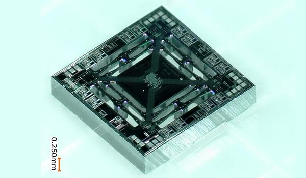
MEMS is a device/system that combines mechanical elements such as actuators and sensors with electronic circuits on a semiconductor substrate. It is manufactured using the same process as semiconductor chips, but with the difference that the 3D structure is built using a more complex process.
This section presents the MEMS manufacturing process.
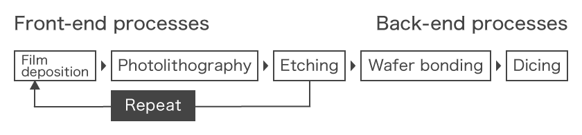
MEMS Manufacturing Flow
In MEMS manufacturing, complex structures are built by repeating the processes from film deposition to etching, which are the front-end processes.
Film Deposition
Film deposition is the process of creating a layer of circuit material on a semiconductor substrate, such as silicon, to form a wiring film or an insulating film.
There are various methods of film deposition, including:
The chemical vapor deposition (CVD) method, in which special gases are fed onto the wafer surface and heat, plasma, or other energy is applied to create a layer;
The sputtering method, in which ions are bombarded onto the material to be formed into a film and the resulting fine particles are used to form the film; and
The thermal oxidation method, in which the wafer is placed in a processing chamber containing oxygen and other gases to oxidize its surface and form a film.
Photolithography
Photolithography refers to the process of drawing patterns on a substrate using light.
A photosensitive resin called a photoresist is applied to the thin film formed in the film deposition process, and the required pattern is drawn using mainly ultraviolet light. The pattern formed by this photoresist serves as a mask material in the subsequent etching process.
There are two types of photoresists: a negative type, in which the light-irradiated area remains, and a positive type, in which the irradiated area is broken down and removed. The specific resist type used varies depending on the application.
Etching
The etching process removes unnecessary portions on the wafer after photolithography. In this process, unwanted portions of the substrate are removed using gas or chemicals. There are two types of etching methods: wet etching, which is performed in a chemical solution, and dry etching, which uses gases and other agents. There are also sacrificial layer etching, deep trench etching, and other types of etching methods, which are used according to the purpose of the MEMS to be manufactured. One of the key differences between MEMS and semiconductor manufacturing processes is the etching process.
Sacrificial Layer Etching
Sacrificial layer etching is mainly used in surface micromachining. In photolithography (patterning), which is a pre-process for etching, a sacrificial layer is formed that functions as a spacer as well as a structure. The sacrificial layer is then scraped away in the etching process to form a moving 3D structure or similar object.
Silicon oxide is generally used as the sacrificial layer, which is often etched using hydrogen fluoride (HF) aqueous solution or hydrogen fluoride (HF) vapor.
Deep Trench Etching
Deep trench etching is also called deep RIE or high aspect ratio (HAR) etching. In the deep trench etching process, a structure is built up by etching deeply into the substrate. Since deeper etching is required for MEMS, a technique to perform deep trench etching while repeating a process of etching and etching sidewall protection is also utilized. In this technique, a protective film is created to suppress etching in the lateral direction, enabling deeper etching.
Wafer Bonding
Wafer bonding is a term that means connection, attachment, or joining, and as suggested by the meaning of the term, it is a process of joining wafers or dissimilar materials together. In the MEMS manufacturing process, this is called substrate bonding, and there are two methods: direct bonding and anodic bonding.
In direct bonding, polished silicon substrates or silicon oxide coated substrates are stacked on top of each other and bonded together using intermolecular forces through heat treatment.
Anodic bonding, on the other hand, is a method of joining glass and silicon substrates by aligning their planes and applying a voltage of several hundred volts.
Both methods are used in MEMS manufacturing, but the anodic bonding method is more commonly used.
Dicing
In semiconductor manufacturing, the process of separating chips formed on a wafer is called dicing.
The dicing process is also used in MEMS. However, the typical dicing method of cutting a wafer with a rotating blade while spraying water may damage the internal structure of MEMS, and so in these cases, a laser is used instead.
Laser Ablation Dicing
The laser ablation method uses a laser beam to process the wafer surface. Since the laser beam cuts without applying pressure from the outside, there is less damage and almost no effect on the internal structure, compared to dicing that uses a circular blade or water pressure to cut.
However, the laser ablation process generates microscopic processing debris. To resolve this problem, a stealth dicing process has recently been introduced, in which a laser with a wavelength that is transparent to the target material is applied to form a modified layer inside the substrate, and then the material is broken into pieces along the cracks that are created, and this technique is sometimes used in MEMS manufacturing.