Technology behind MEMS
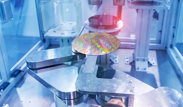
MEMS is found in a wide variety of digital products, including smartphones. We will present here some of the technologies closely related to MEMS manufacturing that support product miniaturization and power saving.
What Is Micromachining?
Micromachining uses semiconductor processing technology to create complex three-dimensional (3D) features, such as structures, sensors, and actuators that make up MEMS, on a substrate.
There are two types of techniques: surface micromachining and bulk micromachining.
MEMS Technology
Surface Micromachining
Surface micromachining is a technique of building up layers on a substrate to create a 3D structure. Sacrificial layers called spacers, which will later be removed, are formed to create beam-like structures. This method is used in the manufacture of integrated MEMS with electronic circuits.
Although the structures are relatively unbreakable, there are some issues when removing the sacrificial layer in that the structures are sometimes attracted to and stick to the substrate when certain chemicals and gases are used.
Bulk Micromachining
Bulk micromachining is a technique that utilizes crystal anisotropic etching and other technologies to deeply carve into wafers to create structures for various mechanical elements. The process was first developed to engrave the substrate using chemicals. Later, the invention of a technique for vertically carving silicon made it possible to process with even greater degrees of freedom.
While this technique allows a high degree of freedom in processing, its disadvantage is that it is easily damaged, which is an issue for future development.
Major Technologies Used in MEMS Manufacturing
There are several technologies used in the manufacture of MEMS that are not commonly used in typical semiconductors and integrated circuits. This section describes some of these characteristic technologies.
Crystal Anisotropic Etching
Silicon crystals have a diamond-like structure, with each crystal plane having a different bonding. Crystal anisotropic etching is a technology that uses these differences to create various shapes.
Crystal anisotropic etching involves deeply dissolving and scraping silicon substrates along their crystal planes with an aqueous alkaline solution. It is widely used for precision processing to create a desired shape according to the mask pattern, and it does not require special manufacturing equipment.
Isotropic Etching
Isotropic etching is an etching technique in which etching proceeds in the horizontal direction in addition to the vertical direction, resulting in a trapezoidal shape of the film directly under the resist.
Isotropic etching uses an etchant made by mixing hydrofluoric acid (HF) and nitric acid (HNO3) and diluting the fluonitric acid with acetic acid. Etching speed is controlled by the etchant concentration, hydrofluoric acid mixing ratio, temperature, and other factors. The advantages of this technique are that inexpensive equipment can be used and multiple wafers can be processed at once.
Isotropic etching is often used to remove the sacrificial layer because it can etch from any direction using chemicals or gases.
Anodic Bonding
Anodic bonding is a technique in which the polished surfaces of glass and silicon substrates are placed on top of each other, and a voltage is applied to the pair while heating to form a strong bond. It is widely used as a bonding technology to create 3D structures for MEMS because it can be performed in air, has a low bonding temperature, and causes little dimensional change.
In recent years, to achieve higher performance in semiconductor components including MEMS, chips and other components are being stacked three-dimensionally for higher density mounting. Anodic bonding is used not only for MEMS packaging and bonding with different materials, but also as one of the stacking technologies that support higher performance in MEMS.