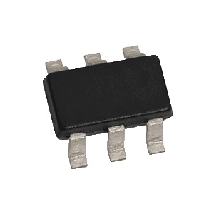
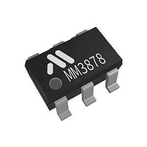
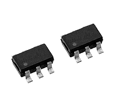
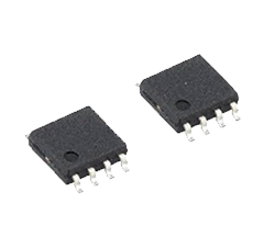
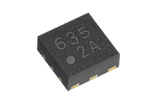
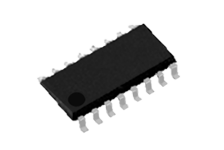
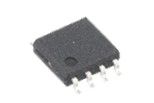
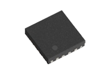
This IC contains two operational amplifiers and achieves extremely low offset voltage with a single power supply. The input offset voltage and the temperature drift of the input offset voltage of these amplifiers are one digit less than those of our conventional products.
Outline
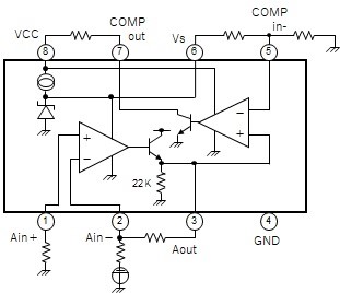
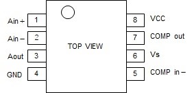
This IC contains an operational amplifier and a comparator, achieving extremely low offset voltage with a single power supply. Since a single power supply can be used, this IC can be operated with the voltage from two batteries. Through the use of the operational amplifier and the comparator, this IC can amplify thermocouple electromotive force and detect ignition according to output from the amplifier, without using other parts. The low offset voltage improves accuracy of ignition detection.
-
-
1.Equipment requiring flame detection, such as gas stoves and water heaters
2.Amplification and detection of very low voltage -
(Unless otherwise specified, Topr = +25℃)
General
1.Power supply voltage........................1.8 to 6.0 V (Suitable for battery-powered devices)
2.Current consumption.........................0.1 mA Typ.
3.Power supply line rejection ratio (PSRR)...60 dB Typ.
Amplifier section
1.Input voltage range.........................-0.2 to 0.3 V
2.Input offset voltage........................±0.1 mV Typ.
3.Gain........................................100 dB Typ.
Comparator section
1.Input voltage range.........................0 to VCC-1.0 V
2.Input offset voltage........................±0.1 mV Typ. -
scroll
Power
supply
voltage
lower limit
[V]Power
supply
voltage
upper limit
[V]Input voltage range
lower limit
[V]Input voltage range
upper limit
[V]Input offset voltage
Typ.
[mV]Temperature drift of
input offset voltage
Typ.
[μV/°C]Gain
Typ.
[dB]Comparator Input
voltage range
lower limit
[V]Comparator Input
voltage range
upper limit
[V]Comparator Input
offset voltage
Typ.
[mV]1.8 6.0 -0.2 0.3 ±0.1 ±1 100 0 VCC-1.0 ±0.1
-
-
Featured Products
Reasons why MinebeaMitsumi semiconductors are the choice
We provide high-performance semiconductors with an integrated system covering development, design, and manufacturing.
Engineering Information
Basic Knowledge
Product Topics
Industry
Contact Us
Please click the inquiry type below according to your question. Each product / sales representative will respond to you.
