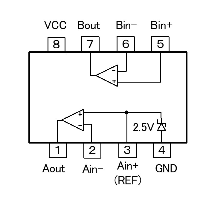
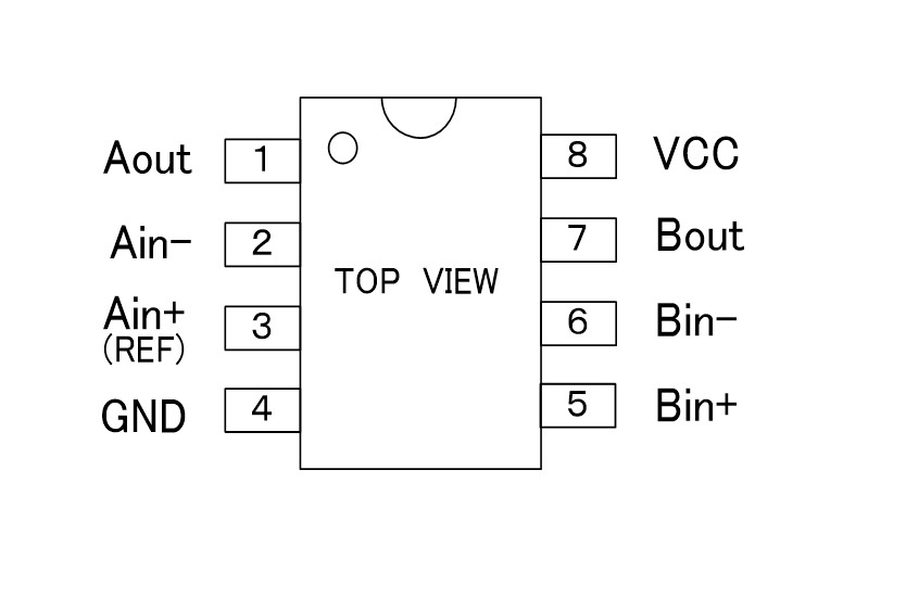
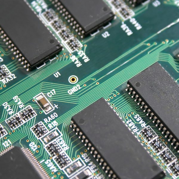
This IC contains two operational amplifiers and achieves extremely low offset voltage with a single power supply. The input offset voltage and the temperature drift of the input offset voltage of these amplifiers are one digit less than those of our conventional products.
Outline
This IC comes with dual operational amplifiers and shunt regulator (2.5V) function.
It can be used for controlling the secondary side of AC adaptor.
It can also be used in a part of application circuit of our IC MM3460 for LED light.
-
-
1. Li-ion battery charger
2. AC adaptor
3. Reference voltage source -
Op-amp unit
1. Input offset voltage Typ.0.2mV, Max0.9mV
2. Input bias current 30nA
3. Power supply current 0.6mA
4. Voltage gain 100dB
5. Common-mode signal rejection ratio 85dB
6. Power supply voltage rejection ratio 100dB
7. Output outflow current 35mA
8. Output inflow current 20mA
Shunt regulator unit
1. Reference voltage 2.5V
2. Minimum cathode current 0.4mA
3. Dynamic inpedance 0.4Ω -
scroll
Power
supply
voltage
lower limit
[V]Power
supply
voltage
upper limit
[V]Input voltage range
lower limit
[V]Input voltage range
upper limit
[V]Input offset voltage
Typ.
[mV]Gain
Typ.
[dB]2.0 20.0 0.0 VCC-1.0 ±0.2 100
-
-
Featured Products
Reasons why MinebeaMitsumi semiconductors are the choice
We provide high-performance semiconductors with an integrated system covering development, design, and manufacturing.
Engineering Information
Basic Knowledge
Product Topics


Industry
Contact Us
Please click the inquiry type below according to your question. Each product / sales representative will respond to you.