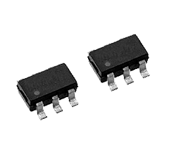
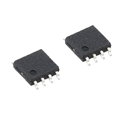
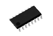
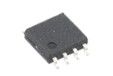
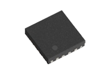
Lithium-Ion Battery protection IC using high voltage CMOS process for overcharge, overdischarge and overcurrent protection of the rechargeable Lithium-ion or Lithium-polymer battery. The overcharge, overdischarge, discharging overcurrent, charging overcurrent, and short protection of the rechargeable Lithium-ion or Lithium-polymer battery can be detected. Each of these IC composed of four voltage detectors, short detection circuit, reference voltage sources, oscillator, counter circuit and logical circuits.
Outline
The MM3625 series are secondary protection IC using high
voltage CMOS process for overcharge protection of the
rechargeable lithium–ion or lithium–polymer battery. The high accuracy overcharge detection of each cell ofthe rechargeable 3,4 cell Lithium-ion or Lithium-polymer battery is possible.The IC has a regulator and it ispossible to stop regulator by
detected overdischarge.The internal circuit of IC is composed by the voltagedetector, the reference voltage source, delay time control circuit, the logical circuit, and regulator circuit etc.
-
-
For 3 to 4 cells secondary protection
-
(1) Range and accuracy of detection/release voltage
● Overcharge detection voltage 3.6V to 4.5V, 5mV steps Accuracy±25mV
● Overcharge release voltage 3.4V to 4.5V, 50mV steps Accuracy±50mV
● VOU OFF voltage 2.1V to 3.2V, 10mV steps Accuracy±50mV
(2) Range and accuracy of detection/release delay time
● Overcharge detection delay time time1ms to (1ms×2n1)+(1ms×2n2)+(1ms×2n3) Accuracy±25%
● Overcharge release delay time 1ms to (1ms×2n1) Accuracy±25%
● VOUT OFF delay time 1ms to (1ms×2n1)+(1ms×2n2)+(1ms×2n3) Accuracy±25%
*n1,n2 and n3 can select arbitrary integers between 0 to 17. (However n1≠n2≠n3)
(3) Range and accuracy of regulator output voltage
● VOUT pin output voltage 1.8V to 5.0V, 50mV steps Accuracy±100mV
(4) The setting for three cell and for four cell protection can be set with the SEL pin
(5) Regulator output can be control with the EN pin
(6) FUSE pin can control with the CTL pin
(7) Low current consumption
● Current consumption1(VDD pin) Vcell=3.5V Typ. 4.5μA Max. 6.5μA
● Current consumption1(VDD pin) Vcell=2.5V Max. 0.1μA(When starting conditions of VOUT are EN pin.)
Max. 1.0μA(When starting conditions of VOUT are cell voltage. -
Click the arrow icon in the table below to switch from ascending to descending order.
scroll
Product
namePackage
Latch function
Overcharge
detection
voltage
[V]Overcharge
release
voltage
[V]VOUT
OFF voltage
[V]VOUT pin
output
voltage
[V]Overcharge
detection
delay time
[s]Overcharge
release
delay time
[ms]MM3625A01RRE PLP-10A 〇 4.425 2.750 2.900 4.100 MM3625A02RRE PLP-10A 〇 4.300 2.500 3.300 4.100 MM3625B02RRE PLP-10A 4.450 4.250 2.500 3.300 4.100 16.0 MM3625B03RRE PLP-10A 4.450 4.250 2.750 3.300 7.170 16.0 MM3625B04RRE PLP-10A 4.500 4.300 2.750 3.300 7.170 16.0 MM3625Y01RRE PLP-10A 〇 4.425 2.750 2.900 4.100 MM3625Z01RRE PLP-10A 〇 4.425 2.750 2.900 4.100 -
Associated Data
Featured Products
Reasons why MinebeaMitsumi semiconductors are the choice
We provide high-performance semiconductors with an integrated system covering development, design, and manufacturing.
Download
Product Topics
Industry
Contact Us
Please click the inquiry type below according to your question. Each product / sales representative will respond to you.
